CXMT's 4F² Memory Gambit Exposes a Costly Split in Global DRAM Strategy
While Micron and rivals pursue 6F² scaling, the Hefei chipmaker is banking on an architecture American firms rejected - a choice driven as much by export controls as engineering.
A Fork in the Road for Memory Density
ChangXin Memory Technologies, the Hefei-based chipmaker that accounts for the bulk of China's domestic DRAM capacity, is pushing forward with a cell architecture that its American and South Korean competitors abandoned years ago. The firm plans to ship samples of server-grade dynamic random-access memory built on a 4F² design before the close of this year, according to statements from the company. That decision places CXMT on a different technical trajectory from Micron, Samsung, and SK hynix, all of whom have standardised on 6F² layouts for current and next-generation products.
The divergence is more than academic. 4F² cells - where "F" denotes the minimum feature size a fabrication process can reliably print - pack transistors and capacitors more tightly than 6F² designs, promising higher bit density per square millimetre of silicon. In theory, that translates to lower cost per gigabyte. In practice, the tighter geometry brings yield challenges, process complexity, and reliability questions that have deterred the industry incumbents from committing capital to the approach at scale.
At Opentechwire, we have tracked memory roadmaps across Northeast Asia for the past three years, and this is the first time a major producer has committed to volume 4F² production for the data-centre segment. The move is a calculated wager that China's relative isolation from leading-edge lithography tools - a direct consequence of US export restrictions tightened in 2022 and again in 2023 - can be offset by squeezing more performance out of mature process nodes through architectural ingenuity.
Why the Incumbents Chose 6F²
The 6F² cell became the de facto standard in the mid-2010s because it balanced density gains with manufacturability. Each memory cell uses six times the square of the minimum feature dimension, leaving enough margin for the capacitor structures that store charge and the access transistors that read or write data. Yields climb faster, defect rates stay manageable, and the resulting chips meet the endurance and refresh-rate specifications that hyperscale data centres demand.
Micron's decision to bypass 4F² was driven by precisely those trade-offs. Engineers at the Boise-based firm concluded that the additional process steps required to etch smaller capacitor trenches and maintain acceptable leakage currents would erode the cost advantage that higher density promised. Samsung and SK hynix reached similar conclusions, opting instead to push 6F² cells to smaller nodes - 1-alpha, 1-beta, and beyond - using extreme ultraviolet lithography where export rules permit.
CXMT, by contrast, lacks unfettered access to EUV scanners. The Netherlands-based ASML, which holds a monopoly on EUV equipment, has not shipped a machine to a Chinese customer since Washington tightened multilateral controls. That leaves the Hefei operation dependent on deep ultraviolet immersion steppers and multi-patterning techniques, both of which favour tighter cell layouts to achieve competitive bit densities without the resolution boost that EUV provides.
The Engineering and Economic Calculus
A 4F² architecture compresses the capacitor and transistor footprint, but it also demands more precise alignment across successive lithography passes and thinner dielectric films to prevent charge leakage. These requirements push up the number of mask layers and lengthen cycle times in the fab, raising the cost per wafer start even as the cost per bit falls. The net outcome depends on yield - the percentage of dies on each wafer that pass final test.
Industry data suggests that 6F² DRAM manufactured on a 1-alpha-nanometre-class node achieves yields in the low-to-mid 80 per cent range within the first year of volume production. Early 4F² efforts at research fabs have historically landed 10 to 15 percentage points lower, though yield curves improve over time as process engineers refine deposition and etch recipes. CXMT has not disclosed projected yields for its server product, but the decision to sample by year-end implies confidence that the line is approaching commercial viability.
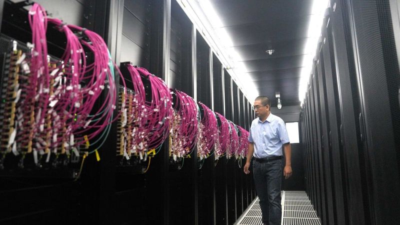
The Hefei site operates fabs that were equipped with DUV tools purchased before the most recent round of controls took effect. By pairing those tools with domestic deposition and metrology systems - some developed by state-backed equipment firms, others licensed or reverse-engineered from Japanese and European designs - CXMT has assembled a process flow that avoids explicit US dependencies. The 4F² cell is a natural fit for that toolset, extracting maximum density from each lithography generation without requiring the wavelength shrinkage that EUV delivers.
Market Positioning and Customer Appetite
Server DRAM is a high-margin segment, with modules typically selling for double the price of equivalent consumer parts. Hyperscalers and cloud infrastructure operators prioritise capacity, bandwidth, and power efficiency, but they also scrutinise supply-chain resilience. The concentration of advanced DRAM production in South Korea - Samsung and SK hynix together command roughly 70 per cent of the global market - has prompted some buyers to seek alternative sources, particularly for secondary tiers of their fleets where cutting-edge performance is less critical.
CXMT has positioned its 4F² offering as a "good enough" alternative for workloads that do not require the absolute lowest latency or highest transfer rates. Internal presentations reviewed by industry analysts suggest the company is targeting DDR5 modules with speeds in the 4,800 to 5,600 megatransfers-per-second range, a step behind the 6,400 MT/s and faster parts that Micron and Samsung are ramping for AI training clusters, but adequate for general virtualisation, storage controllers, and edge inference boxes.
The question is whether data-centre operators will accept chips from a supplier whose technology path diverges from the rest of the ecosystem. Qualification cycles for server memory run six to nine months, and any hint of elevated failure rates or refresh anomalies can disqualify a vendor for years. CXMT's sampling schedule suggests it is aiming for initial deployments in the second half of next year, assuming customers validate performance and reliability.
Geopolitical Pressure and Industrial Policy
Behind the technical narrative lies a strategic imperative. Beijing has designated memory semiconductors as a national priority, funnelling subsidies and policy support to CXMT and its smaller peer, Fujian Jinhua, in an effort to reduce dependence on imports. DRAM accounts for roughly 15 per cent of China's total semiconductor import bill, a figure that has climbed as domestic AI and cloud infrastructure expands.
Export controls have made that goal harder to reach. By restricting access to EUV lithography and certain categories of process-control equipment, Washington has effectively capped the node at which Chinese fabs can operate without smuggling or sanctions evasion. The 4F² architecture is CXMT's answer: a design that wrings more capability out of the tools it can legally procure, even if the resulting process is more complex and the margins thinner.
US policymakers, for their part, view memory as a dual-use technology with implications for military and intelligence systems. DRAM is ubiquitous in everything from missile guidance to signals processing, and any attempt by China to achieve self-sufficiency in the category is seen through a security lens. The result is a feedback loop in which tighter controls push Chinese firms towards novel architectures, which in turn prompt calls for further restrictions on the ancillary tools and materials those designs require.
What Comes Next
If CXMT's 4F² server DRAM proves viable in volume production, it will mark the first time in a decade that a major memory architecture has forked along geopolitical lines. The 6F² standard emerged from a consensus among Samsung, SK hynix, Micron, and the now-defunct Elpida and Qimonda, all of whom shared access to the same equipment vendors and process know-how. A parallel 4F² ecosystem, confined largely to China and the customers willing to qualify it, would represent a fragmentation of the global memory supply chain with implications for interoperability, pricing, and long-term R&D investment.
For the broader semiconductor industry, the episode underscores how export controls can reshape not just market access but the fundamental design choices that companies make. When leading-edge tools are unavailable, engineers optimise for different variables - tighter cells instead of finer lithography, more mask layers instead of EUV simplicity, domestic supply chains instead of global best-of-breed. The trade-offs are real, the costs are measurable, and the outcomes remain uncertain.
CXMT's gambit will be tested in the fabs and data centres over the next 18 months. If yields climb and customers adopt, the 4F² path could become a template for other Chinese chipmakers navigating similar constraints. If the architecture stumbles, it will stand as a reminder that technical ambition alone cannot overcome the physics and economics that drove the rest of the industry in a different direction.