China's 3-nm Chip Push Advances Without EUV Access
Researchers achieve early progress in sub-3-nanometre processing using older lithography tools, charting alternative route around US export controls
An Alternate Route Takes Shape
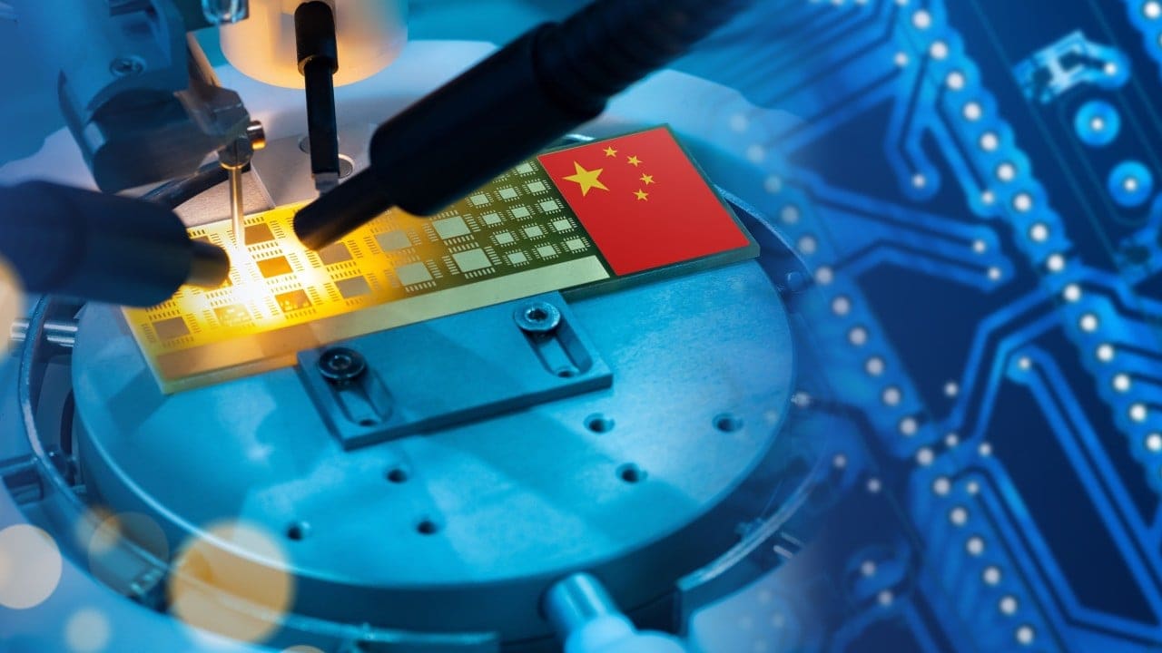
Researchers in China have demonstrated early progress in fabricating semiconductor devices at processing nodes below 3 nanometres without access to the most advanced lithography equipment. The work relies on older deep ultraviolet (DUV) technology rather than the extreme ultraviolet (EUV) systems that foundries elsewhere use for cutting-edge production.
ASML, the Dutch equipment manufacturer, remains barred from shipping its EUV lithography machines to China under export control regimes coordinated by Washington. Those restrictions, which tightened across 2023 and 2024, have forced Chinese semiconductor organisations to explore workarounds that trade process simplicity and yield for capability.
At Opentechwire, we've tracked the evolution of these constraints closely. The current approach represents a gamble: whether multiple exposures, tighter process tolerances, and novel patterning techniques can substitute for hardware that the global industry considers essential for nodes below 5 nm.
The Technical Leap
Moving to 3-nm-class nodes without EUV requires a technique called multi-patterning, in which DUV tools expose the same layer of photoresist multiple times to achieve feature densities that would otherwise demand shorter wavelengths. The method increases cycle time, raises defect risk, and complicates mask alignment, but it is not theoretically impossible. Taiwan and South Korea employed similar strategies at 7 nm and 5 nm before EUV became economically viable for high-volume manufacturing.
What makes the Chinese effort notable is the compression of the development timeline. Organisations working on these processes have had to iterate without the supplier ecosystem, process libraries, and institutional knowledge that TSMC and Samsung accumulated over years of EUV deployment. Early strides, according to researchers involved, include test wafers demonstrating transistor densities consistent with 3-nm design rules, though yield rates and power characteristics remain undisclosed.
The work does not yet constitute production readiness. Achieving a few functional die on experimental wafers is separate from running a stable, economically viable manufacturing line. The gap between laboratory demonstration and commercial-scale output has historically taken years to bridge, even with full access to leading-edge tools.
Policy and Industrial Pressure
Export controls on semiconductor equipment have been a centrepiece of US technology policy towards China since 2018, but the restrictions have intensified significantly in recent years. The October 2022 rules from the Bureau of Industry and Security expanded controls beyond EUV to include advanced DUV immersion systems, deposition tools capable of supporting sub-14-nm production, and software used in electronic design automation.
The effect has been to draw a technological perimeter around China's semiconductor sector. Companies such as SMIC, the country's largest foundry, have found themselves unable to procure replacement parts for some existing equipment, let alone acquire next-generation systems. The restrictions also extend to personnel: US nationals and green-card holders are prohibited from supporting certain Chinese fabs without a licence.
These measures reflect a broader strategic calculation in Washington. Semiconductors underpin not only consumer electronics but also data-centre infrastructure, telecommunications equipment, and defence systems. Denying China access to the most advanced nodes, the reasoning goes, limits the performance ceiling of systems built on domestically produced chips.
Beijing, in turn, has responded with subsidies, research mandates, and procurement preferences intended to accelerate indigenous capability. The results have been uneven. Progress at mature nodes - 28 nm and above - has been substantial, with Chinese fabs now competitive in automotive, industrial, and consumer applications. At the leading edge, however, the gap remains wide.
Implications for the Foundry Landscape
If Chinese teams can demonstrate stable, reproducible sub-3-nm processes using DUV, the strategic calculus shifts. Yield and cost per wafer would likely remain worse than EUV-based production, but the gap might narrow enough to support domestic demand in applications where performance, not margin, is the priority. Military, aerospace, and surveillance systems fall into that category.
For the global foundry industry, the scenario introduces a bifurcation. TSMC and Samsung would continue to serve customers requiring the highest transistor density and energy efficiency, using EUV for 3-nm, 2-nm, and eventually sub-2-nm nodes. Chinese fabs, operating under export controls, would serve a separate market with lower performance but adequate capability for a range of applications.
That bifurcation carries risks. A parallel supply chain insulated from Western technology could eventually develop its own equipment base, reducing long-term leverage for export controls. Alternatively, the technical and economic costs of operating without EUV could prove prohibitive, leaving Chinese fabs structurally disadvantaged.
The outcome will depend in part on how quickly Chinese researchers can move from early test wafers to volume production, and whether the cost and yield penalties of multi-patterning can be managed at scale. It will also depend on the durability of the export control regime itself. If restrictions ease, the incentive to pursue a parallel path diminishes. If they tighten further, the pressure to succeed intensifies.
What Comes Next
The semiconductor industry has long operated on the assumption that leading-edge manufacturing requires a globalised supply chain: lithography tools from the Netherlands, deposition systems from the United States, materials from Japan, and design software from California. Export controls have tested that assumption by forcing one major economy to attempt self-sufficiency at the frontier.
Early progress on sub-3-nm nodes without EUV suggests that the technical barriers, while high, are not insurmountable. Whether the economic and operational barriers can be overcome remains an open question. The answer will shape not only China's semiconductor trajectory but also the structure of the global industry for the next decade.